- PG Admissions 2023 Announced
- | Ph.D. Admissions 2023 Announced
- | Admission Helpline - Voice call: 080 66 91 91 80
- M.Tech. (EC) - last date 28th April 2022
- Admission Helpline - Voice call: 080 66 91 91 80
- UG Admissions - All India Category - Admission Status Announced
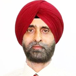
Harpreet Singh Jattana

Contact Details
Biography
Have hands-on experience (more than 37 years) in the following areas of microelectronics:
CMOS Process development and Integration (SOI, HV, BiPolar, NVM, OTP)
VLSI Design for Space/Military applications
Radiation hardened Technology for VLSI products.
CMOS fabrication and Mass production
Device reliability and failure modes
IC testing, characterization, Packaging and Qualification
Failure Analysis of CMOS
Project planning, execution and Management
Materials management, procurement.
Equipment specifications formulation, technical comparison
ToT related issues – Device types, process details, unit recipes, Tech vehicle, IPs, design flows etc.
MEMS Cantilever and Z-measurement MEMS device for Biomedical applications
Subject Knowledge & Understanding
Non conventional MOS devices
Lower Node Technology (incl products and markets)
VLSI Packaging ( Ceramic, Plastic, Small-outline, 2D, MCM,2.5D)
MEMS Design
MEMS Fabrication (Surface & Bulk Micromachining, LEGA)
Compound Semiconductors (GaN, GaAs based devices)
Medical Devices
Clinical Validation
Teaching Semiconductor courses (MTech, BTech )
Specialization
CMOS Process Development, Device Reliability, CMOS Design, Compound Semiconductors, VLSI Testing & Packaging, Wafer Fabrication
Publications
| Sr No. | Title | Journal | Month and Year |
|---|---|---|---|
| 1 | L style n- MOSFET Layout for Mitigating TID Effects | Springer http://doi.org/10.1007/s12633-021-01150-z |
May 2021 |
| 2 | Effect of optical parameters on design of highly reflecting distributed Bragg reflectors based on compound semiconductors for space applications | Material science http://doi.org/10,1007/s12034-021-02356-y |
March 2021 |
| 3 | Transient response of 0.18mm SOI MOSFETS and SRAM bit-cells to heavy-Ion irradiation for variable SOI film thickness. | IEEE Transactions on Electron Devices | Vol 66 No.11, Nov 2018 |
| 4 | A physics based variability –aware methodology to estimate critical charge for near-threshold voltage latches. | IEEE Transactions on Electron Devices | Vol 27 No.9 Sept 2019 |
| 5 | Source Underlap – A novel technique to Improve sate operating area and output-conductance in LDMOS transistors | IEEE Transactions on Electron Devices | Vol 66, No. 11 Nov 2019 |
| 6 | Addressable Synchronous Asynchronous Differential Receiver Design in 0.18um CMOS | ISED 2021 | 2021 |
| 7 | Development of Low cost Silicon BJT Technology and Modelling | ICEE 2020 at IIT Delhi | Dec 2020 |
| 8 | SPICE Based compact modelling of a spiral Inductor and MIM capacitor for RF circuit simulations | ICEE 2020 at IIT Delhi | Dec 2020 |
| 9 | Modeling of 0.18mm RF Bulk and SOI Planar MOSFETs using Industry Standard BSIM Models | ICEE 2020 at IIT Delhi | Dec 2020 |
| 10 | Verilog – A SPICE Model of PECVD SiO2 OTP Memory Device | IEEE International Conference on modelling of systems circuits and Devices | Jan 2019 |
| 11 | Hi Rel ASIC Design and Development – A case study | IEEE International Conference ICECA | Jan 2018 |
| 12 | Technology development of High Gain BJT to enable 180nm BiCMOS technology | IWPSD | Oct 2017 |
| 13 | Simple PE CVD SiO2 OTP memory based PUF for 180nm node for IoT. | 75th Annual Device research Conference DRC | Jan 2017 |
| 14 | Comparative Simulation Analysis of Process Parameter Variation in 20nm Triangular FinFET | Active and Passive Electronic Components Journal | Oct 2017 |
| 15 | Design & Development of High Speed LVDS Receiver with Cold-Spare | VDAT, Communications in Computer and Information Science | July 2016 |
| 16 | Accurate analysis of settling error in CDS Integrator based Sigma Delta Modulator, | IEEE INDICON International Conference | Sept 2015 |
| 17 | SCL 180nm CMOS Foundry – High Reliability ASIC design for aerospace applications | 19th VDAT | May 2015 |
| 18 | Design, Implementation and Performance Evaluation of LVDS Transmitter | Journal of Spacecraft Technology | July 2014 |
- 21 Technical papers in “Compendium of Research work “(ISRO)
- Accurate analysis of settling error in CDS integrator based Sigma delta modulator INDI-CON 2015
- Simple PE CVD SIo2 OTP Memory based PUF for 180nm node for IOT: 75th Annual de-vice research conference DRC
- Technology development of high gain BJT 180nm BiCMOSTechnology : IWPSD 2017
- IEEE Transactions on Electron Devices page 4826, Vol 66 Nov 2018.Number 11: Transi-ent response of 0.18 um SOI MOSFETS and SRAM bit-cells to heavy-ion Irritation for variable SOI film thickness.
Conference Proceedings:
- 21 TECHNICAL PAPERS IN “COMPENDIUM OF RESEARCH WORK “(ISRO)
Teaching
Have taught the following courses to MTech/PhD /Btech students at IIST Trivandrum, Manipal University Jaipur, EICT IIT Guwahati, WPU Pune, NIRMA University and MNIT Jaipur
- Device Physics
- CMOS Analog Design
- VLSI Microfabrication
- VLSI Digital design, including Low Power design
- Design of Data Converters (ADCs, DAC, PGA)
- Physical design Implementation
- Device Modelling, characterization and Failure modes of MOS Tx

